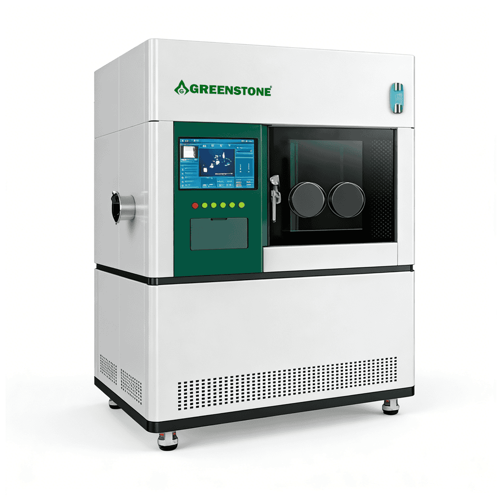
Prezentarea caracteristicilor echipamentului
The FE-SEM integrates a Schottky Field Emission Electron Gun, livrarea ≤1 nm resolution și 0.1–30 kV acceleration voltage for nanoscale to microscale imaging. With a 15,000+ hour source lifetime și auto beam alignment, it enables direct imaging of non-conductive samples at ≤5 kV without coating. Equipped with a 5-axis motorized stage (supports 200 mm samples) and multi-mode detectors (SE/BSE/EDS), this system excels in high-throughput analysis for materials science, life science, and semiconductor industries, ensuring precision for both research and quality control.
Why Choose Our FE-SEM?
- Nanoscale Precision: Unmatched resolution for cutting-edge research and industrial QA.
- Adaptive Workflows: From conductive metals to delicate biological samples, all in one system.
- Future-Ready: Modular design supports upgrades (e.g., cryo-stage, 3D EBSD).
probe prelucrate

Avantaje cheie
1. High-Performance Schottky Field Emission Electron Gun
- Ultra-High Brightness: Delivers exceptional brightness of 10⁹ A/(sr·m²·V) with energy spread <0.3 eV and probe size ≤1 nm, ensuring sub-nanometer resolution.
- Extended Source Life: Operational lifespan exceeds 15,000 hours, minimizing downtime.
- Low-Voltage Excellence: Achieves <1 nm resolution at 0.1–30 kV, ideal for beam-sensitive and non-conductive samples.
2. Superior Stability & Analytical Versatility
- Stabilitatea grinzii: Beam current drift <0.5%/hour for reliable long-duration analysis (e.g., CL, EDS, EBSD).
- Non-Conductive Sample Compatibility: Direct imaging of uncoated samples (polymers, biological tissues) at ≤5 kV without gold sputtering.
3. User-Centric Design
- Smart Automation: Features auto beam alignment, one-click workflows, and touchscreen controls for seamless operation.
- Large Sample Capacity: Accommodates specimens up to 200 mm in diameter with an optional 5-axis motorized stage (tilt ±90°, rotate 360°).
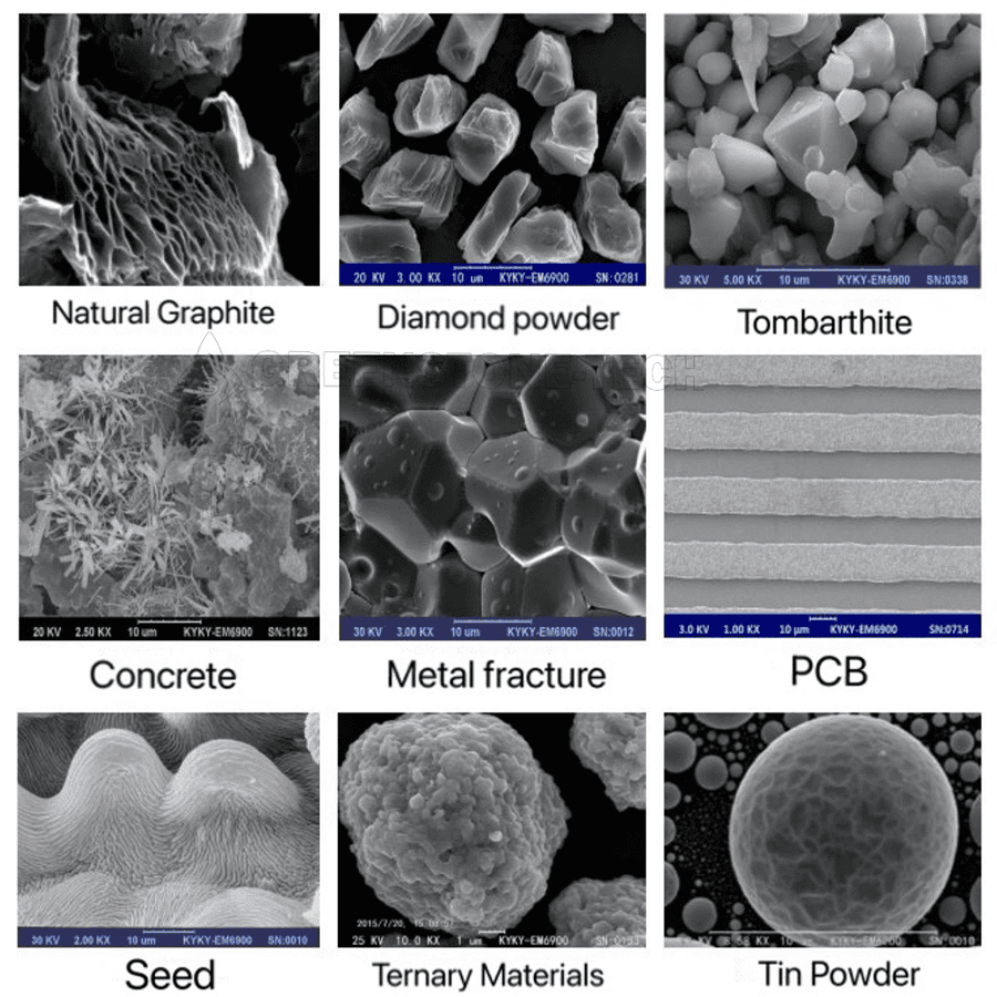
Aplicații
| Field | Key Applications |
|---|---|
| Materials Science | Nanostructure morphology, fracture analysis, thin-film interfaces |
| Life Science | Cellular ultrastructure, viral particle imaging (cryo-prepared) |
| Geoscience | Mineral phase mapping, pore structure characterization |
| Semiconductor QA | Defect inspection, photoresist profiling, nanowire metrology |
| Forensics & Industry | Trace evidence analysis (fibers, particulates), PCB solder joint evaluation |
Technical Specifications
| Parametru | Specificații |
|---|---|
| Electron Source | Schottky Field Emission Gun |
| Rezoluție | ≤1.0 nm (at 15 kV), ≤1.4 nm (at 1 kV) |
| Acceleration Voltage | 0.1–30 kV |
| Vacuum Modes | High Vacuum: 10⁻⁴–10⁻⁵ Pa; Low Vacuum: 10–100 Pa (for uncoated samples) |
| Detectors | SE, BSE, EDS (optional WDS, CL, EBSD) |
| Sample Stage | 5-Axis Motorized Stage: X/Y 110 mm, Z 50 mm, Tilt ±90°, Rotate 360° |
| Chamber Size | 200 mm (diameter) × 80 mm (height) |
Articolul | GST32-SEM1000 (FE SEM Scanning Electron Microscope) |
Rezoluție | 1nm@30kv(SE) 3nm@1kv(SE) 2.5nm@30kv(BSE) |
Magnification | 6X~1000,000X |
Electron gun type | Schottky field fires electron guns |
Accelerating voltage | 0~30kv |
Automatic function | Focus, brightness/contrast, astigmatism, medium electron beam pair |
Vacuum system | 1 ion pump, 1 getter ion compound pump, 1 molecular pump and 1 mechanical pump |
Detector | High vacuum secondary electron detector (with the protection for the detector) |
Sample stage | Five-axis automatic pre-centering sample stage |
Travel range | X: 0~150mm |
Y: 0~150mm | |
Z: 0~60mm | |
R: 360° | |
T: -5°~70° | |
Maximum sample diameter | 340mm |
Optional detector | BSE/EDS/EBSD/CL |
Optional accessories | Pre-drawing roomEBLhigh and low temperature tablenano consolestretching tablehand control boxtrackball |
Produse conexe
Stăpânirea tehnologiilor de bază în fabricarea aditivă a metalelor de înaltă performanță și tratarea suprafețelor