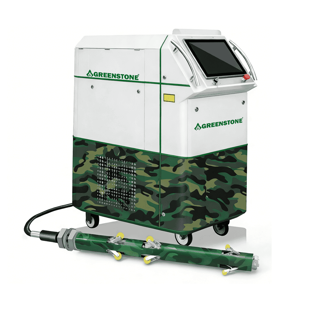
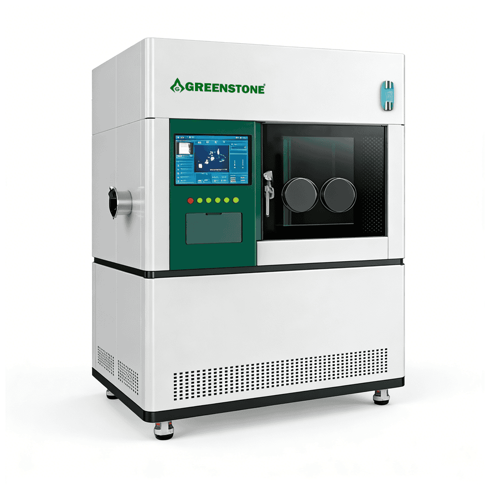
GSTHBC350A Κεραμική επεξεργασία λέιζερ ινών (σκληρός και εύθραυστος εξοπλισμός κοπής λέιζερ κεραμικού υλικού)
Παρουσίαση των χαρακτηριστικών του εξοπλισμού
Fiber laser ceramic processing equipment is specially developed for cutting hard and brittle ceramic materials. It has outstanding advantages in the processing of alumina, aluminum nitride silicon nitride, zirconium oxide ceramics and sapphire materials; the main technical advantages are: the side of the line is neat and clean without residue; it can quickly punch small holes with a diameter of less than 0.15mm; the heat-affected area is small and there is no cracking due to heat.
επεξεργασμένα δείγματα


- Small spot size enables high-quality, high-efficiency and high-processing;
- Small thermal impact, low requirements for raw material selection;
- Automatic loading and unloading, assisted by machine vision to achieve automatic calibration and alignment, fully automated operation;
- Supports DXF graphics import, which can meet the layered processing of any basic graphics.
| Παράμετρος | Αξία |
| Platform Movement Range (mm) | 350×350 |
| Maximum Processing Size (mm) | 300×250 |
| Punching Efficiency (/s) | ≥8(Φ[email protected]@S2mm) |
| Scribing Speed (mm/s) | 10–200 |
| Minimum Hole Diameter (mm) | Φ0.04 |
| Platform Positioning Accuracy (μm) | ±3 |
| Repeat Positioning Accuracy (μm) | ±2 |
| Hole Taper (μm) | ≤±20 (middle [email protected]) |
| Minimum Cutting Line Width (μm) | 30 |
| Cutting Thickness (mm) | ≤2 |
| Equipment Size (mm) (W×D×H) | 1440×1400×2000 |
| Equipment Weight (kg) | 1650 |
Laser cutting solution Overview: Compared with traditional industrial cutting methods, laser cutting effectively reflects the processing advantages of photon manufacturing such as high precision and flexibility. It is widely used for precision cutting in the electronics field, such as consumer electronics, automotive electronics, communication electronics, etc.
| Εικόνα αποτελεσμάτων | Περιγραφή |
 | Connector Material Bridge Cutting: The single-side material bridge cutting time (0.2mm thick copper nickel/tin-plated) is 0.12s. High efficiency meets standard production line CT requirements, with no carbonization and no burrs. OS yield rate is greater than 99%. SI testing shows no defects. |
 | In-Vehicle Camera Low-Temperature Welding: The weld seam width is 0.7mm, penetration depth is 0.4mm, and the efficiency reaches 10mm/s. The welding temperature is below 60℃, with a clean appearance, no oxidation blackening, and no spatter. |
 | DPC Circuit Board Cutting: The cutting efficiency for a 0.5mm thick board is 20mm/s, while for a 1mm thick board, it is 5mm/s. Dimensional accuracy reaches ±20μm, and the scribing half-cut efficiency is 200mm/s. |
 | PCB QR Code Marking: The QR code is of Grade A with an engraving size accuracy of ±0.05mm. The laser spot is uniform and round, and the background pattern is clear. |
 | PCB Carbon-Free Cutting: The cutting speed for a 2mm thick PCB board is 25mm/s, with an accuracy of ±20μm. The heat-affected zone is less than 20μm, and the edges remain carbon-free. |
 | MinLED Backplane Carbon-Free Cutting: The cutting speed for a 1.6mm thick board is 25mm/s, with an accuracy of ±20μm. The heat-affected zone is less than 20μm, and the edges remain carbon-free. |


Σχετικά προϊόντα
Κατακτώντας τις βασικές τεχνολογίες στην προσθετική κατασκευή μετάλλων υψηλής απόδοσης και στην επεξεργασία επιφανειών